Huawei Unveils Tau (τ) Scaling Law for Transistor and System Breakthroughs
Huawei has introduced the Tau (τ) Scaling Law at the 2026 IEEE International Symposium on Circuits and Systems, proposing a new approach to semiconductor development. This law aims to replace traditional geometric scaling with time scaling to enhance transistor density and performance. The company has already produced 381 chips based on this principle and plans to launch Kirin chips featuring the LogicFolding architecture in Fall 2026.
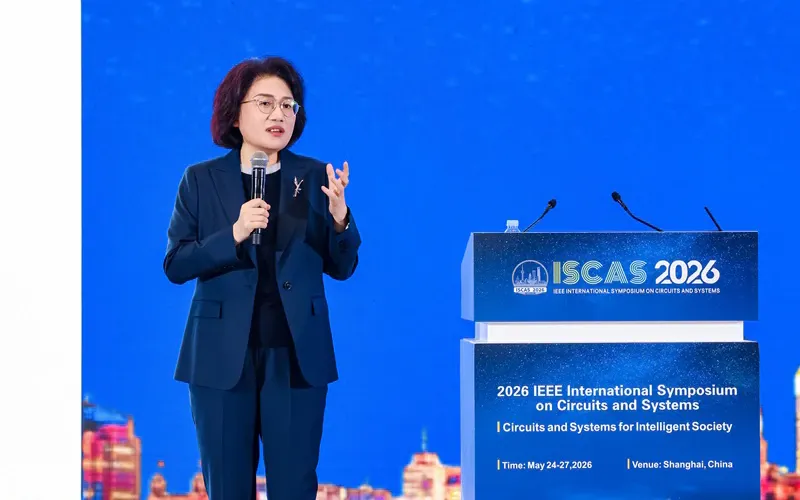
- ▪He Tingbo from Huawei presented the Tau (τ) Scaling Law as a new guiding principle for the semiconductor industry.
- ▪The τ Scaling Law focuses on time scaling rather than geometric scaling to improve semiconductor performance.
- ▪Huawei has designed and mass-produced 381 chips based on the τ Scaling Law, with plans for Kirin chips to launch in Fall 2026.
Opening excerpt (first ~120 words) tap to expand
[Shanghai, China, May 25, 2026] Today, at the 2026 IEEE International Symposium on Circuits and Systems (ISCAS), He Tingbo from HUAWEI delivered a keynote speech titled "New Semiconductor Path in Practice". In her speech, she presented the Tau (τ) Scaling Law, a new principle for guiding the future development of the semiconductor industry. This law proposes replacing geometric scaling with time (τ) scaling as a new guiding principle for the evolution of both semiconductors and electronic systems. Based on this principle, innovative technologies such as LogicFolding can be used to continuously compress signal propagation delay and steadily improve transistor density, which will drive the ongoing evolution of semiconductors and electronic systems.
…
Excerpt limited to ~120 words for fair-use compliance. The full article is at Huawei.
Discussion
0 commentsMore from Huawei


