Huawei announced it will have a 1.4nm equivalent density process by 2031
Huawei has announced plans to achieve a 1.4nm equivalent density process by 2031, utilizing a new technology called Logic Folding. This approach aims to enhance performance and reduce latency without relying on EUV technology. The company emphasizes collaboration and innovation in the semiconductor industry to drive sustainable development.
- ▪Huawei plans to implement a 1.4nm equivalent density process by 2031, just three years behind TSMC.
- ▪The Logic Folding technology aims to reduce internal circuitry length, improving performance and cutting latency.
- ▪Huawei has designed and mass-produced 381 chips over the past six years based on the Tau Scaling Law for various applications.
Opening excerpt (first ~120 words) tap to expand
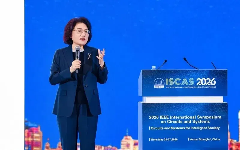
Huawei looks to 1.4nm by 2031 This morning Huawei announced it will have a 1.4nm equivalent density process in place by 2031 – only three years behind TSMC – without using EUV. At the 2026 IEEE International Symposium on Circuits and Systems (ISCAS) in Shanghai, Huawei semiconductor president He Tingbo (pictured) delivered a speech titled “New Semiconductor Path in Practice” and said the company has developed a process called ‘Logic Folding’ by which it reduces the length of internal circuitry thereby cutting latency and improving performance.
…
Excerpt limited to ~120 words for fair-use compliance. The full article is at Electronicsweekly.
Discussion
0 commentsMore from Electronicsweekly